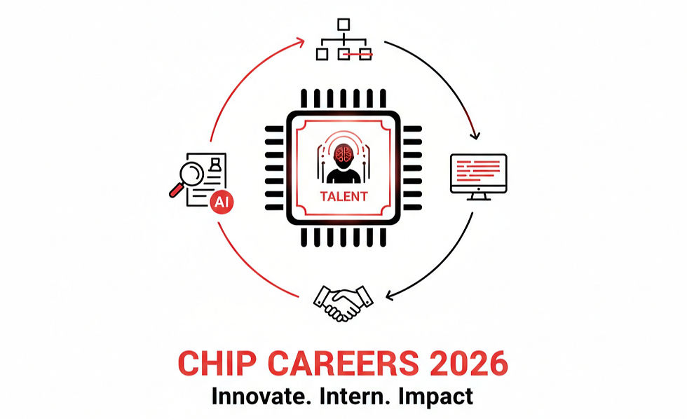
Breaking into Silicon: How Chip Companies Hire Interns in 2026
- Feb 17
- 4 min read
The semiconductor industry is no longer just about hardware; it is the heartbeat of the global economy. As we move through 2026, the demand for high-performance computing, AI-integrated circuits, and sustainable energy solutions has pushed semiconductor giants like Intel, NVIDIA, TSMC, and AMD to rethink their talent pipelines. If you are an engineering student wondering how chip companies hire interns today, you are looking at a landscape defined by hyper-competition, AI-driven screening, and a massive focus on "full-stack" hardware expertise.
In this guide, we will break down the evolving recruitment cycle, the technical hurdles of the modern interview, and the specific strategies you need to secure a seat at the table in 2026.
How Chip Companies Hire Interns - A Million Opportunities
The semiconductor sector is projected to create over 1 million jobs globally by the end of 2026. With the rise of the India Semiconductor Mission (ISM) and similar initiatives in the US and EU, the "talent crunch" is real. Companies are no longer just looking for "graduates"; they are looking for "interns who can contribute to tape-outs."
Understanding how chip companies hire interns in this high-stakes environment requires looking past the job portal and into the strategic shifts of 2026, where "skills-based hiring" has officially replaced "prestige-based hiring."
1. The Timeline: When Does the Hunt Begin?
In 2026, the hiring cycle has become year-round, but the "Big Peak" remains. To stay ahead, you must understand the two primary windows:
The Summer Peak (May – August Internship): Applications open as early as September of the previous year. By February 2026, most top-tier firms like TSMC and Samsung have already moved into the interview phase.
The Off-Season/Co-op Window: Companies now offer 6-month "working student" or co-op roles (common at NXP and Infineon) that start in January or September.
Phase | Timeline | Action Item |
Early Bird | Sept – Nov | Resume tailoring & Portfolio building |
Peak Application | Dec – Feb | Active applying & Referral hunting |
Interview Season | Jan – May | Technical drilling & Coding tests |
Onboarding | June – July | Documentation & Relocation |
2. The Multi-Stage Interview Process
The standard "two-round" interview is a relic of the past. In 2026, how chip companies hire interns involves a rigorous, four-to-five-stage gauntlet designed to test both theoretical depth and practical adaptability.
Stage 1: AI-Powered Resume & Portfolio Screening
Most resumes are now parsed by AI tools that look for specific EDA (Electronic Design Automation) tools and process nodes. If your resume doesn't mention 7nm or $5nm$ flows, or tools like Cadence Virtuoso and Synopsys PrimeTime, it might never see a human eye.
Stage 2: The Implementation-Heavy Online Assessment (OA)
Unlike standard software roles, semiconductor OAs in 2026 are "implementation-heavy." You won't just solve a LeetCode Medium; you might be asked to:
Write modular SystemVerilog or Verilog for a specific state machine.
Solve a 3-part problem where Part 1 must work to unlock Part 2 (a trend popularized by companies like Stripe and now adopted by Meta and Nvidia).
Perform basic Tcl or Python scripting for flow automation.
Stage 3: The Technical Deep-Dive (The "Whiteboard" Round)
This is where the real filtering happens. Expect questions on:
Computer Architecture: Cache coherence, pipeline hazards, and RISC-V vs. ARM.
VLSI Fundamentals: Setup/Hold time violations, $NMOS$ vs. $PMOS$ switching speeds, and CMOS inverter characteristics.
Power Optimization: Clock gating, multi-threshold voltage cells, and power-aware design.
Stage 4: The Integration & "Real-World" Round
Some companies now provide access to a private GitHub repo or a simulated EDA environment. They want to see how you handle "Production-Ready" code. Can you document your RTL? Is your verification environment scalable?
3. Skills in High Demand for 2026
To truly master the process of how chip companies hire interns, you need to align your skill set with the "New Big Three" of the 2026 chip world:
AI Hardware Acceleration: Knowledge of how to optimize GPUs and TPUs for machine learning workloads.
Verification (UVM/SystemVerilog): 60% of design time is now spent on verification. If you know UVM (Universal Verification Methodology), you are a gold-tier candidate.
Physical Design & DFT (Design for Test): Understanding synthesis, PnR (Place and Route), and how to make a chip testable post-manufacturing.
Expert Tip: "Readability is King." In 2026, recruiters at firms like ARM and Meta prioritize clean, modular code over "clever" one-liners. Use descriptive variable names; x or temp will get you rejected.
4. The Rise of "Human Skills" in Engineering
A surprising trend in 2026 is the focus on Soft Skills. With cross-functional teams (Designers working with Fab engineers and Software teams), companies are using AI-driven assessments to measure:
Emotional Intelligence (EQ): How do you handle a bug that delays a tape-out?
Adaptability: Can you switch from 28nm legacy nodes to 2nm cutting-edge tech?
Communication: Can you explain a complex timing violation to a non-technical project manager?
5. Regional Hubs: Where to Apply
While Silicon Valley remains the heart, 2026 has seen the rise of massive global hubs:
India (Bengaluru, Gujarat): The new manufacturing and design frontier.
Taiwan (Hsinchu): The undisputed king of fabrication (TSMC).
Europe (Finland, Germany): Focus on automotive chips (Nordic Semi, Infineon).
FAQ: Understanding the 2026 Intern Hiring Process
Q: How chip companies hire interns in 2026 compared to 2020?
A: In 2026, the process is much more specialized. While 2020 focused on general engineering principles, 2026 hiring is "skill-centric." Companies look for specific experience with EDA toolchains, advanced nodes (sub-7nm), and AI-optimized architectures. The use of AI screening and collaborative coding platforms has also made the process faster but more competitive.
Q: Is a high GPA required for semiconductor internships?
A: Most giants like Samsung and Intel still prefer a 3.0 or 3.5+ GPA, but they are increasingly flexible if you have a "taped-out" student chip or a significant GitHub contribution to open-source hardware like RISC-V.
Q: Are these internships paid?
A: Yes. In 2026, almost all technical internships in this sector are paid, often with high stipends (ranging from ₹15-20 lakh per year equivalent in India to $7,000+ per month in the US) plus relocation and housing assistance.
Conclusion: Your Next Steps
Understanding how chip companies hire interns is only half the battle; the other half is execution. The 2026 market is hungry for talent, but only for those who can bridge the gap between classroom theory and clean-room reality.
Would you like me to review your resume and suggest specific semiconductor keywords to bypass AI filters for your 2026 applications?


Comments